ELECTRON SHOWER: THE FUTURE OF MICROCHIP MANUFACTURING
A revolutionary method called the “electron shower” is changing the way microchips are made. This new technique uses controlled electron cascades to improve the process of creating thin films, which are vital layers in electronic devices. With this development, scientists and engineers are hopeful that microchips can be manufactured faster, cheaper, and with greater precision.
What is the “Electron Shower” Technique?
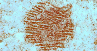
The term “electron shower” might sound like something from science fiction, but it refers to a real scientific process. In this method, a focused beam of electrons is directed onto a material. These high-energy electrons then strike atoms in the material, knocking out other electrons. This creates a cascade, or a “shower,” of electrons spreading through the material. This shower helps deposit or modify ultra-thin layers-called thin films-on microchips.
This method allows for better control over the material properties. It also ensures that the film layers are more even and compact, which is essential for microchips to work efficiently.
Why Thin Films Matter in Electronics
Thin films are extremely small layers-sometimes just a few atoms thick-applied to the surface of a microchip. These films can act as conductors, insulators, or semiconductors depending on the material used. They are essential in transistors, sensors, solar panels, displays, and other electronic components.
Traditionally, thin films are made using processes like chemical vapor deposition (CVD), physical vapor deposition (PVD), or sputtering. However, these methods can be expensive, time-consuming, and less precise. This is where the electron shower technique stands out as a game-changer.
How It Works: Simple Explanation
Here’s a step-by-step of how the electron shower method works:
Targeting: A beam of electrons is aimed at the material surface in a vacuum chamber.
Impact: These electrons collide with the atoms of the material.
Cascade Begins: The impact causes a chain reaction where many more electrons are released.
Layer Formation: These electrons help spread and deposit the film evenly over the surface.
Control and Precision: The whole process is closely monitored and controlled, ensuring a smooth, ultra-thin, high-quality layer.
This method is especially useful when working with very delicate or sensitive materials, such as those used in next-generation chips.
Benefits of the Electron Shower Technique
Greater Precision: The method allows fine-tuning of the film’s thickness and composition at the atomic level.
Faster Production: Since the film can be deposited more quickly and evenly, production times are reduced.
Lower Costs: With fewer steps and less material waste, the overall manufacturing cost goes down.
Eco-Friendly: The process uses fewer chemicals and creates less waste, making it better for the environment.
Compatibility: It can work with a wide range of materials, including metals, oxides, and semiconductors.
A Step Forward for the Semiconductor Industry
The semiconductor industry is always looking for ways to pack more power into smaller chips. With the demand for smaller, faster, and more energy-efficient electronics growing rapidly, traditional methods are reaching their limits. The electron shower technique could help break these limits.
This method could play a big role in producing advanced processors, memory chips, flexible electronics, and even quantum computing components. It also opens the door for improvements in industries like renewable energy (solar panels), medical devices, and telecommunications.
Challenges and Future Outlook
While the technique is promising, it still faces challenges:
Scalability: Can this method be used on a large industrial scale?
Cost of Equipment: Advanced electron beam systems are still expensive to build and maintain.
Training and Expertise: Engineers and technicians need specialized training to operate and maintain these systems.
Despite these hurdles, many experts believe that continued research and investment will overcome them. Already, several research labs and companies are experimenting with pilot projects to integrate electron shower techniques into commercial chip production.
Conclusion
The “electron shower” technique could revolutionize microchip manufacturing by making it faster, cheaper, and more precise. By using controlled electron cascades to enhance thin-film creation, it provides a more efficient and eco-friendly way to build the tiny layers that power today’s electronics. As the world becomes more digital and connected, innovations like this will be essential in keeping up with the demand for smarter, smaller, and more powerful devices. The future of electronics might just begin with a shower-not of water, but of electrons.